Miyajima Group Research
Click on each item to jump to the detailed description.
- Photovoltaic Power Converters for Blue-Light Optical Wireless Power Transmission aiming for Underwater and Long-distance Energy Transfer (Material and Device Development)
- Ultra-low Damage Sputtering Technology and its Applications (e.g., Silicon Solar Cells, Metal Films)
- Quality Improvement of Copper Oxide Materials and Application to Low-Environmental-Impact Solar Cells
- Formation and Evaluation of Quantum-Cutting Phosphor Thin Films and their Application (LSC-type Solar Cells)
● Photovoltaic Power Converters
We are promoting research on next-generation photovoltaic power converters, which are the core of Optical Wireless Power Transmission (OWPT) technology to realize wireless power supply for mobile objects, IoT devices, and underwater equipment. In particular, to efficiently convert monochromatic light such as high-energy-density blue lasers into electricity, we are exploring innovative materials centered on all-inorganic wide-gap perovskites (CsPbBr3-based). From the perspectives of both material science and device physics, we aim to realize the ultimate blue-light power converter with a theoretical efficiency of approximately 70% by utilizing high-quality interface control via low-damage sputtering and heterojunction technology with nitride semiconductors. We conduct integrated research ranging from elucidating the fundamental physical properties of light-absorbing materials to practical device design.
(1) Quality Improvement of Wide-gap Perovskite Materials
Since OWPT uses monochromatic light sources such as lasers and LEDs, receivers must be designed to achieve maximum conversion efficiency at specific wavelengths. The conversion efficiency of a receiver varies depending on the wavelength used. While a receiver can convert light with energy greater than the bandgap of its absorption layer into electrical energy, any excess energy from photons significantly larger than the bandgap is lost as heat. Therefore, conversion efficiency is maximized when the light energy is close to the bandgap of the absorption layer. Furthermore, when using light energy near the bandgap, the theoretical conversion efficiency (assuming ideal device structure and materials) increases as the bandgap of the absorption layer becomes wider. This necessitates receivers using wide-gap materials (though it also requires high efficiency from corresponding short-wavelength light sources). At the Miyajima Lab, we are focusing on perovskite materials, which have gained attention as solar cell materials, and are specifically working on evaluating the photovoltaic power conversion characteristics and improving the quality of CsPbBr3 and CsPb(Br1-xClx)3 .
(2) Photovoltaic Power Converters Using Wide-gap Perovskite Materials
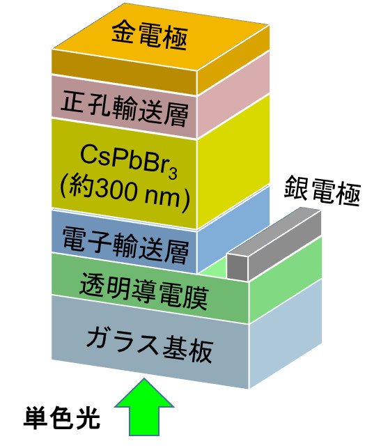
The figure on the right shows a typical structure of a photovoltaic power converter using CsPbBr3, a wide-gap perovskite material, as the light absorption layer. We are conducting studies using nanocrystalline gallium nitride (nc-GaN) as the electron transport layer and P3HT as the hole transport layer, while also searching for materials better suited to the band lineup of CsPbBr3.
We have successfully fabricated devices using nc-GaN and P3HT and confirmed their photovoltaic conversion characteristics. Our research has revealed that the composition adjustment of the CsPbBr3 absorption layer significantly impacts device performance.
Selected Publications:
Murata et al., AIP Advance 10, 045031 (2020)
Aso et al., Jpn. J. Appl. Phys. 62, SK1045 (2023)
Tan et al., Physica Status Solidi A 2400437, (2024)
Watanabe et al., Physica Status Solidi rrl 2500209 (2025)
● SiH4-free Process for High-Efficiency Crystalline Si Solar Cells (from 2012)
In recent years, the installation of solar power generation has grown rapidly, driven primarily by monocrystalline silicon solar cells. With their widespread adoption, manufacturing costs have dropped significantly, and the proportion of cell manufacturing costs within the overall cost of solar power is decreasing. In this context, improving efficiency is just as crucial as further cost reduction. By increasing power generation per unit area through higher efficiency, it is possible to reduce non-cell costs (such as BOS costs). Currently, the mainstream structure for monocrystalline silicon solar cells is the PERC type, but it is approaching its efficiency limit. To achieve further improvements, technologies such as heterojunctions using hydrogenated amorphous silicon (a-Si:H) and passivation contact types (TOPCon) using tunnel oxide films and heavily doped polysilicon layers are being considered. However, these face the challenge of higher manufacturing costs compared to PERC. Therefore, our group is researching cost-reduction technologies for high-efficiency monocrystalline silicon solar cells, specifically focusing on processes that do not use explosive or toxic gases.
(1) Fabrication of High-Quality Amorphous Silicon Surface Passivation Films for Solar Cells via Facing Targets Sputtering
High-efficiency crystalline silicon solar cells utilize heterojunctions with hydrogenated amorphous silicon (a-Si:H) rather than conventional pn junctions formed by thermal diffusion. For these a-Si:H layers, Plasma-Enhanced Chemical Vapor Deposition (PECVD) or Cat-CVD methods are used, as they allow for high-quality thin film deposition at relatively low temperatures (~200°C). These methods decompose monosilane (SiH4) gas using plasma or heated metal catalysts to generate radicals that form the film on the substrate. For p-type and n-type doping, gases containing boron or phosphorus (such as B2H6 or PH3) are added. SiH4 is known to be highly explosive, while B2H6 and PH3 are highly toxic. These are classified as specialized high-pressure gases, requiring expensive abatement and safety equipment to prevent leaks, which increases costs.
To address this, we are investigating methods that do not use these gases—specifically, sputtering. Sputtering involves ionizing an inert gas like Argon via plasma discharge and colliding the ions into a target (the material to be deposited) to deposit the ejected atoms onto a substrate. When fabricating a-Si:H with this method, a silicon target and argon gas mixed with a few percent of hydrogen can be used, eliminating the need for explosive or toxic gases. However, sputtering is rarely used for solar cell-grade a-Si:H due to the damage caused to the silicon substrate (or the film/substrate interface) during deposition, primarily by secondary electrons. To suppress this damage, our laboratory focuses on Facing Targets Sputtering (FTS). We have successfully formed high-quality a-Si:H passivation films for crystalline silicon solar cells using FTS and are currently working on further improving the passivation effect.
Selected Publications:
Shiratori et al., Applied Physics Express 11 031301 (2018)
Faris et al., Progress in Photovoltaics: Research and Applications 28 971 (2020)
Shiratori et al., IEEE Journal of Photovoltaics 10, 927 (2020)
Li et al., Solar RRL 8, 2400045 (2024)
(2) Fabrication Process for TOPCon Solar Cells via SiH4-free Process
TOPCon solar cells have recently attracted attention as a high-efficiency Si solar cell structure. However, their formation process typically requires the use of highly explosive SiH4 and toxic PH3 to form amorphous or polysilicon layers. By using the Facing Targets Sputtering method to form these films with low damage, we aim to manufacture high-efficiency solar cells using a SiH4-free process.
Selected Publication:
Yamaguchi et al., Japanese Journal of Applied Physics 62 SK1024 (2023)
Equipment in Use
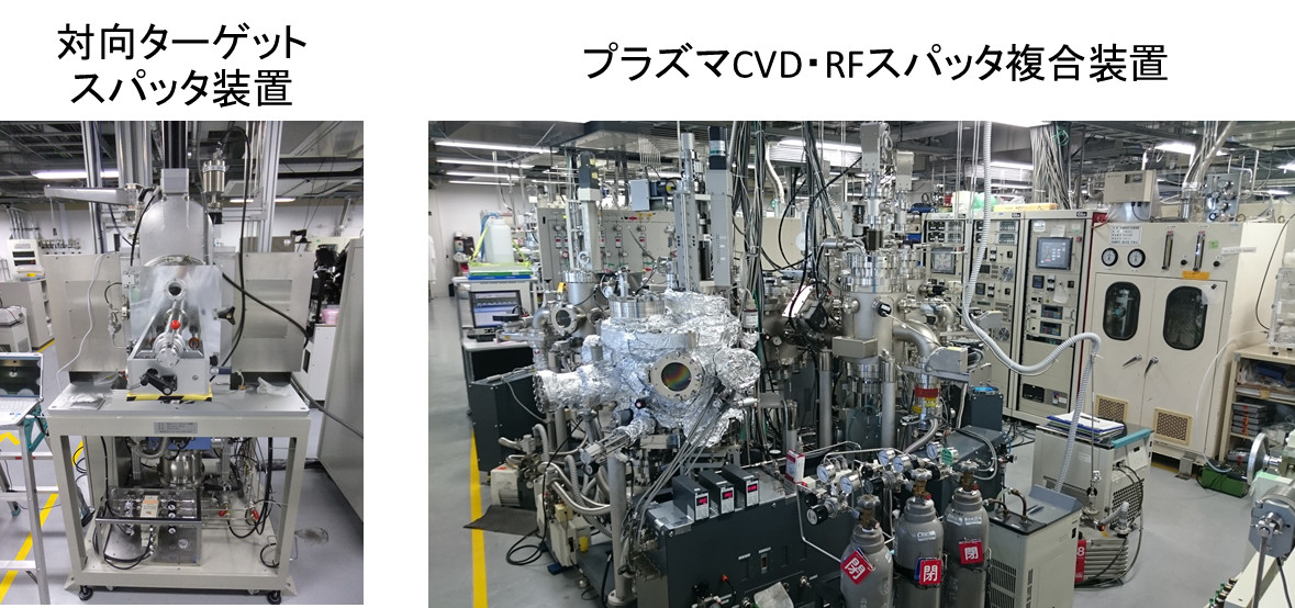
Shown below is the Facing Targets Sputtering (FTS) system used for fabricating hydrogenated amorphous silicon (a-Si:H) passivation films, metal oxide emitter layers, and transparent conductive films for solar cells. The FTS system consists of a load-lock and a main chamber. Three sets of facing target plasma sources are connected to the sides of the main chamber. By rotating the substrate holder in the center, three different materials can be deposited sequentially without removing the sample from the chamber. We also use a standard Plasma CVD (PECVD) system for comparison. This PECVD system consists of a load-lock, a robot transfer chamber, three PECVD chambers, and an RF sputtering chamber, allowing for the deposition of p-type, i-type, and n-type silicon thin films, transparent conductive films, and metal oxides.
● Quality Improvement of Copper Oxide Materials and Application to Low-Environmental-Impact Solar Cells
Under construction
(1) Under construction
Under construction
(2) Under construction
Under construction
● Quantum-Cutting Phosphors and their Applications (from 2025)
This research aims to realize thin films of quantum-cutting phosphors (which convert one high-energy ultraviolet to blue photon into up to two low-energy near-infrared photons) and apply them to Luminescent Solar Concentrator (LSC) type solar cells. To achieve carbon neutrality by 2050, accelerating decarbonization is essential. Particularly in urban areas, buildings account for a large proportion of energy consumption and CO2 emissions, making measures in the architectural field critical. Japan also faces many natural disasters, requiring improved resilience through building-level energy self-sufficiency. Against this background, we aim to add power generation functionality to currently underutilized window surfaces.
(1) Theoretical Study of LSC Solar Cells Using Quantum-Cutting Phosphors
Under construction
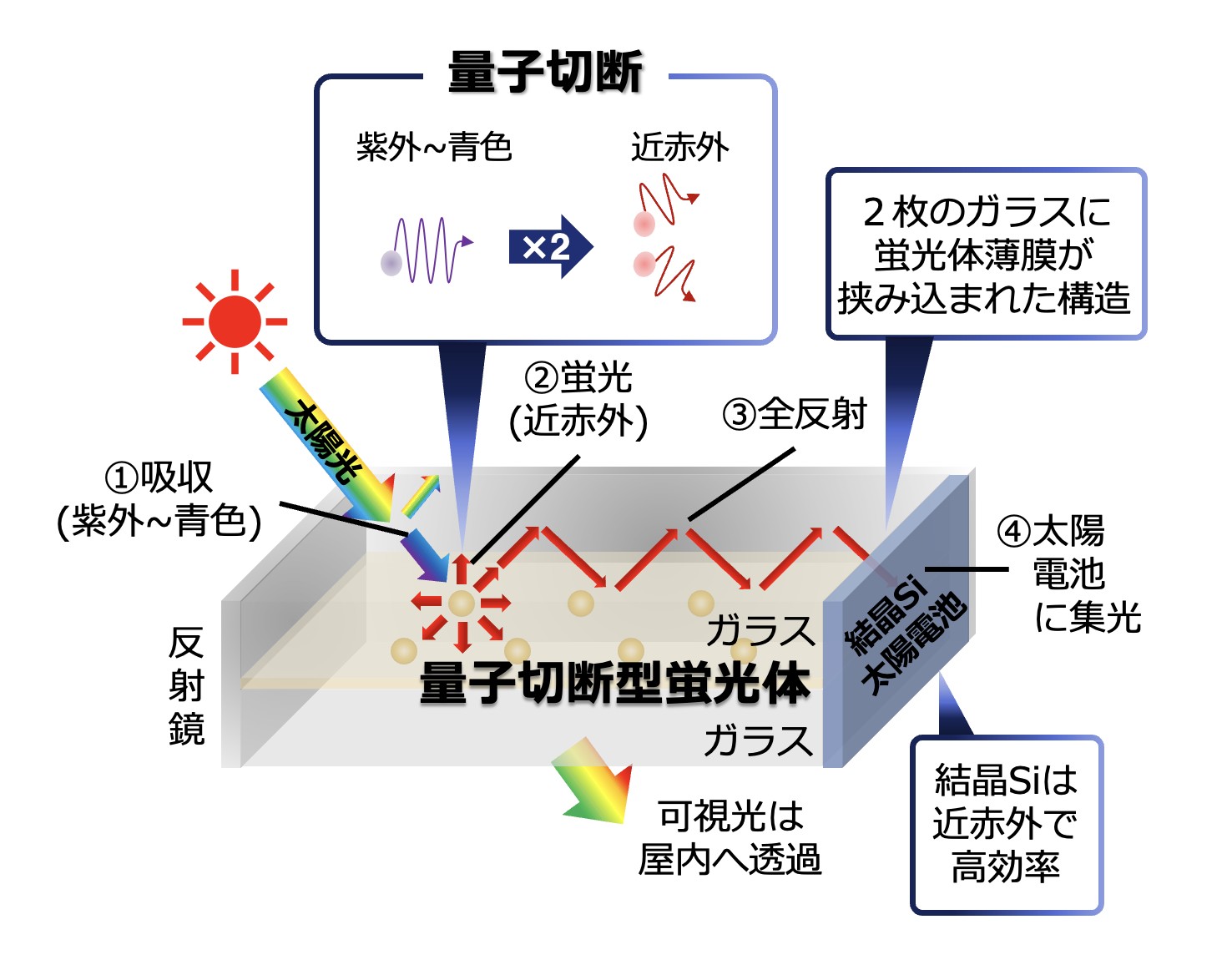
(2) Fabrication of Quantum-Cutting Phosphor Thin Films
LSC technology was proposed in the 1970s, but research temporarily stalled due to issues such as photodegradation of organic phosphors and reabsorption losses, combined with the falling price of silicon solar cells. However, in recent years, performance has improved with the emergence of new materials like quantum dots and perovskites. This, coupled with the rising demand for transparent power-generating devices in architecture, has brought renewed attention to the field. Our laboratory has been developing CsPb(Br1-xClx)3 as a material for optical wireless power receivers. In this research, we leverage this material foundation and aim to realize a Quantum-Cutting Luminescent Solar Concentrator (QC-LSC) by adding Yb3+ to provide quantum-cutting properties. The resulting near-infrared light corresponds to the wavelength range where monocrystalline silicon solar cells have high external quantum efficiency. Furthermore, because it utilizes only wavelength ranges where human visual sensitivity is low, high visible light transparency is expected.